PRODUCTS
Your Expert for
Monolithic Sapphire Ingots
FAMETEC´s ability to grow high-quality 150 and 200 mm diameter crystals along both the a- and c-axis offers exceptional versatility. This, combined with our high yield and minimal waste processes, positions us as an ideal solution for large-scale sapphire wafer production, optoelectronics (LED, MiniLED, MicroLED), power semiconductors, optical applications, and windows or watch glasses.
As a European manufacturer, we offer supply chain stability, close collaboration opportunities, and a strong emphasis on traceability and quality management systems. This ensures the consistent reliability of our sapphire materials.
WAFER
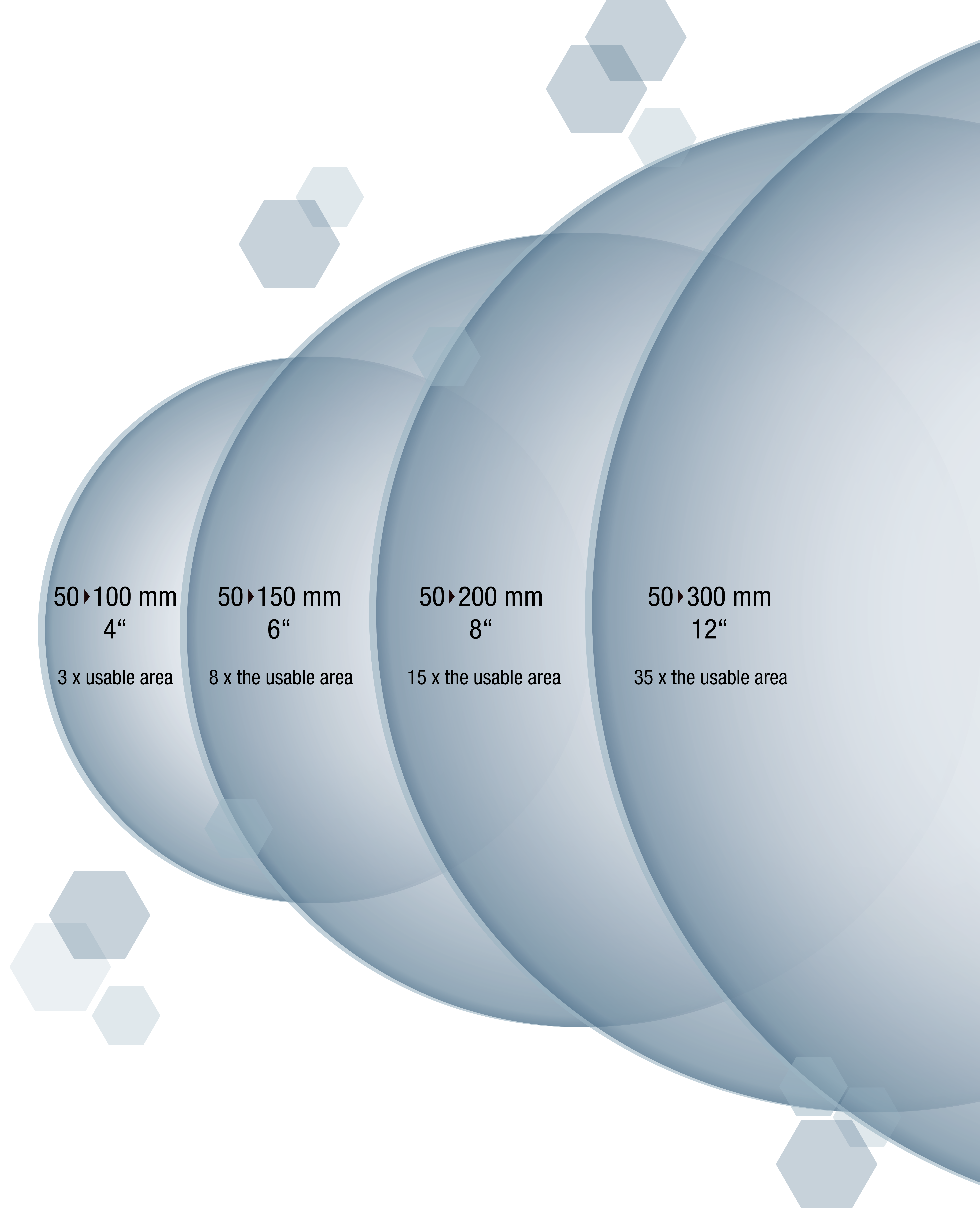
Size matters - why go bigger
Size matters in semiconductor manufacturing, and FAMETEC offers the substrate technology you need. Our ability to grow high-quality crystals along both the a- and c-axis in 150 mm and 200 mm diameters provides immediate benefits. We are also pushing boundaries with the possibility to develop 300 mm, opening the door to even greater efficiency gains.
Advantages of transitioning to larger sapphire wafers:
- Reduced handling and improved economies of scale
- Increased usable area
- Higher yields and lower cost per chip
- Enhanced automation and process control
TWO PATHS TO SAPPHIRE GROWTH
HEM vs. Kyropoulos
HEM was invented in the 1960s. It employs melt growth, with growth taking place upwards, and heat is exchanged with helium gas. The method is fast and economical but produces crystal of low quality and consumes crucibles.The Kyropoulos method was invented in the 1970s. It also employs melt growth, combined with top seeding, pulling and natural cooling.
This method consumes a large amount of power and seeding is carried out manually, which can be time-consuming. However, it produces crystals of good quality and coring has enabled the production of sapphire wafers with diameters of 50 and 100 mm.
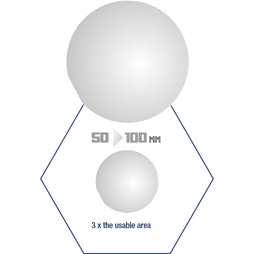
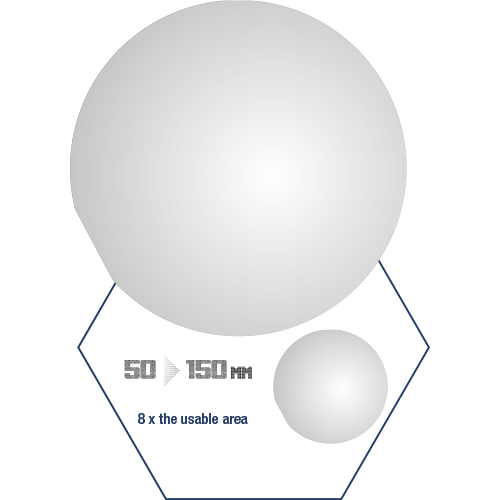
8 x TIMES THE USABLE AREA
50 > 150 mm
FAMETEC‘s McSAP, a modified HEM method introduced in 2012, offers low power consumption, high productivity, semi-automatic growth, and crystal growth along any axis. This directly translates into high-yield ingots, enabling 150, 200, and even 300 mm wafers without the need for perpendicular coring.
McSAP technology revolutionizes sapphire production with zero-emission sapphire semiconductor substrates (ZESSS) that boast superior qualities and yields. These large-diameter ingots are ideal for the semiconductor sapphire substrates employed in applications such as LEDs, miniLEDs, microLEDs and PowerGaN products.
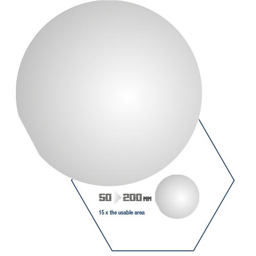
8 x TIMES THE USABLE AREA
50 > 200 mm
The McSAP advantage: Large wafer made possible. McSAP’s ability to grow high-quality crystals along the c-axis, combined with its high yield and minimal waste, makes it the ideal solution for large-scale sapphire wafer production.
This translates directly to FAMETEC‘s ability to offer:
- 150 mm sapphire wafers: currently available and in production
- 200 mm sapphire wafers: available and ready for integration into customer processes
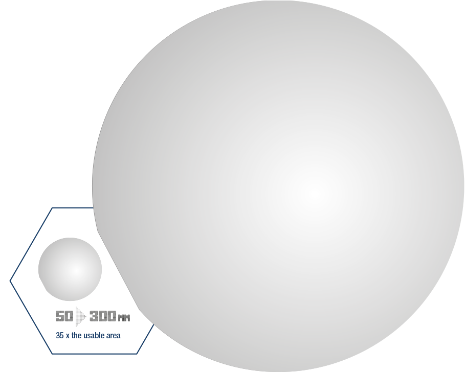
35 x TIMES THE USABLE AREA
50 > 300 mm
If you can dream it, we can do it.
Future-proof technology: McSAP paves the way for the development of even larger wafers up to 300 mm in diameter, further maximizing the benefits in economy and efficiency for chip manufacturers.
APPLICATIONS
Powering the Future with Sapphire Innovation
Mini- and MicroLED Displays
Beyond LEDs: The rise of mini- and microLED displays
LED technology has revolutionized displays, offering energy efficiency alongside excellent image quality. However, advances continue to test its limits. microLED technology has emerged as the next step, promising superior pixel density, contrast ratio, and brightness while maintaining low power consumption. These advantages translate into crystal clear images across various applications, from high-definition TVs to automotive lighting and commercial displays. FAMETEC’s McSAP technology does not just meet industry needs: it also leads to a significant reduction in CO2 emissions throughout the supply chain, due to its energy-efficient production process. This environmental benefit complements the inherent energy savings of microLED displays themselves.
Power Electronics
Power Electronics
PowerGaN technology is experiencing significant growth in high-power electronics applications due to its superior properties, such as high voltage handling and thermal conductivity. This shift is evident as companies move towards GaN-on-sapphire for power devices, particularly with the increasing demand for electric vehicles (EV/HEV) that require efficient power converters and inverters.
FAMETEC is well-positioned to support this transition by providing large-diameter ingots and the essential sapphire substrates used in power electronics.
Optical Applications
Optical Applications
FAMETEC offers a comprehensive selection of a- and c-axis sapphire materials, catering to the diverse needs of the optical market. Our high-purity boules impress by reaching diameters of 210 mm and heights of 220 mm, providing an economical basis for various optical components.
Our large-diameter boules are ideal for the demanding requirements of optical applications. With fully customizable furnaces we can engineer solutions to match any scale you envision, delivering precisely the specifications you need.
Windows and Glasses

Windows and Glasses
FAMETEC’s McSAP technology allows the production of high-purity sapphire, ideal for watch glasses or windows used in defense and other applications due to its scratch resistance and clarity. Its semiconductor grade material is bubble and fog free.
The simultaneous growth of multiple crystals with McSAP leads to a higher yield of usable sapphire material, improving overall production efficiency.
FAMETEC’s expertise in both crystal growth and furnace design allows us to collaborate closely with watch glass or window manufacturers, developing customized solutions for their specific needs.
CONTACT
Get in Touch with Us
You would like to know more about FAMETEC? Our sales team is happy to help you!